Sponsored Link

Sunday, November 23, 2008

Intel® Core™2 Extreme processor QX9770


Intel® Core™2 Extreme processor
For extreme computing. Enjoy revolutionary levels of performance enabling vivid, high-definition experiences and multi-tasking responsiveness from state-of-the-art Intel dual-core and quad-core technologies.

Get untouchable desktop performance from Intel's latest Extreme processor. Play games, edit high definition video and easily tackle the most demanding multitasking environments like never before.

Processor Number

Cache Clock Speed Front Side Bus


45 nm
QX9775¹ 12MB L2 3.20 GHz 1600 MHz


QX9770 12MB L2 3.20 GHz 1600 MHz


QX9650 12MB L2 3.00 GHz 1333 MHz


65 nm
QX6850 8 MB L2 3.00 GHz 1333 MHz


QX6800 8 MB L2 2.93 GHz 1066 MHz


QX6700 8 MB L2 2.66 GHz 1066 MHz


X6800 4 MB L2 2.93 GHz 1066 MHz


Saturday, November 22, 2008

Intel and Clarion gives In-Car Internet Applications


Chrysler announced last week that its UConnect Web in-car Internet service will be available starting August 25 as a dealer-installed option. And at this week's Intel Developer Forum in San Francisco, Intel and Clarion showed applications and products that move us another step closer to the .car era.

An Intel senior VP at IDF showed how Intel and BMW are working together to build a multimedia and computing system for the car that's powered by Intel's powerful Atom chip and provides Internet access. The demo included showing how an on-board computer could use an in-dash monitor to provide GPS navigation data and screens in the backseat would allow passengers to connect to the Internet and watch streaming video.

Clarion used the occasion of IDF to show a production version of its MiND (Mobile Internet Navigation Device) portable nav system that connects to the Internet via WiFi. Clarion claims it will also be able to connect using WiMax and 3G networks in the future. MiND includes software for applications ranging from a Web browser to email as well as viewers for YouTube, MySpace and Google Maps. An integrated Internet search and GPS function also allow local search of area businesses.

The Clarion MiND has a 4.8-inch 800 x 480 pixel touchscreen, a built-in speaker and a rechargeable Li-Ion battery and it also includes an MP3 player and Bluetooth. The unit uses Intel's Atom processor and has 4 GB of flash memory, along with an SD card slot and twin USB ports. The Clarion MiND can also be used as a "portable Internet appliance" in the home or anywhere else, and the device has an "Automobile Mode for safe access behind the wheel," according to CNET.

The Clarion MiND was unveiled at the Consumer Electronics Show in January of 2008, and will be available in the fourth quarter.

Monday, November 17, 2008

INTEL Presents "Classmate PC"


The World Ahead Program from Intel Corporation aims to enhance lives by accelerating access to uncompromised technology for everyone, anywhere in the world. Focused on people in the world's developing communities, it integrates and extends Intel's efforts to advance progress in four areas: accessibility, connectivity, education, and content.

Intel has a long history of working to improve education worldwide and our ongoing programs prepare teachers and students for success in the global economy.

The Intel-based classmate PC is a small, mobile educational solution that Intel has developed specifically for students.

In the past twenty-five years, the popularization of personal computers (PCs) together with access to the Internet has had a profound effect on peoples' lives. However, only roughly 10 percent of current households in the emerging markets of Africa, SE Asia, Latin America, India, China and Russia currently have PCs.

The classmate PC is a revolutionary new device targeted at providing one computing solution per student, taking advantage of the education focus to deliver a product that provides great student education in a rugged industrial design intended for children.


Features


  • Designed for education
  • Durable rugged design for children's day-to-day use
  • Small, kid friendly, form factor for classroom use
  • Easy to carry and light-weight
  • Education-specific features
  • Integrated software and hardware solution
  • Learning through fun, collaboration and interaction
  • Easy to deploy
  • IA-based, runs on already available content, applications and operating systems with full compatibility to standard PC ecosystem

Thursday, October 30, 2008

Intel vPro


Intel vPro technology is a set of features built into a PC’s motherboard and other hardware.Intel vPro is not the PC itself, nor is it a single set of management features (such as Intel Active Management Technology (Intel AMT)) for sys-admins. Intel vPro is a combination of processor technologies, hardware enhancements, management features, and security technologies that allow remote access to the PC -- including monitoring, maintenance, and management -- independently of the state of the operating system (OS) or power state of the PC.Intel vPro is intended to help businesses gain certain maintenance and servicing advantages, security improvements, and cost benefits in information technology (IT) areas.

Relationships between Intel vPro, Intel AMT, Intel Centrino 2, and Intel Core 2

The numerous Intel brands can be confusing. Here are the key differences between vPro (a platform), AMT (a technology), Centrino 2 (a package of technologies), and Core 2 (a processor).

Intel Core 2 Duo or Quad processors are central processing units (CPUs), the brains of the PC.Intel Centrino 2 processor technology is a package of technologies that includes the Intel Core 2 Duo.Intel Centrino 2 is designed for mobile PCs, such as laptops and other small devices. Core 2 and Centrino 2 use 45-nm nanotech manufacturing processes, have multi-core processing, and are designed for multithreading.

Intel vPro technology is a set of technologies built into the hardware of the laptop or desktop PC.The technology is targeted at businesses, not consumers. A PC with vPro includes Intel AMT, Intel Virtualization Technology (Intel VT), Intel Trusted Execution Technology (Intel TXT), a gigabit network connection, and so on. You can have a PC with a Core 2 processor, without vPro built in. However, vPro features require a PC with at least a Core 2 or Centrino processor. Current versions of vPro are built into PCs with Core 2 Duo or Quad processors or Centrino 2 processors.

Intel AMT is part of the Intel Management Engine, which is built into PCs with Intel vPro technology.Intel AMT is a set of remote management and security features designed into the PC’s hardware and which allow a sys-admin with AMT security privileges to access system information and perform specific remote operations on the PC.These operations include remote power up/down (via wake on LAN), remote / redirected boot (via integrated device electronics redirect, or IDE-R), console redirection (via serial over LAN), and other remote management and security features.

Thursday, October 16, 2008

Intel 805xx product codes

Product code Marketing name(s) Codename(s)
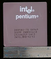
80500 Pentium P5 (A-step)
80501 Pentium P5
80502 Pentium P54C, P54CS
80503 Pentium with MMX Technology P55C, Tillamook
80521 Pentium Pro P6
80522 Pentium II Klamath
80523 Pentium II, Celeron, Pentium II Xeon Deschutes, Covington, Drake
80524 Pentium II, Celeron Dixon, Mendocino
80525 Pentium III, Pentium III Xeon Katmai, Tanner
80526 Pentium III, Celeron, Pentium III Xeon Coppermine, Cascades
80528 Pentium 4, Xeon Willamette (Socket 423), Foster
80529 Celeron Timna (canceled)
80530 Pentium III, Celeron Tualatin
80531 Pentium 4, Celeron Willamette (Socket 478)
80532 Pentium 4, Celeron, Xeon Northwood, Prestonia, Gallatin
80533 Pentium III Coppermine (cD0-step)
80535 Pentium M, Celeron M 310-340 Banias
80536 Pentium M, Celeron M 350-390 Dothan
80537 Core 2 Duo T-series, Celeron M 5xx Merom
80538 Core Solo, Celeron M 4xx Yonah
80539 Core Duo, Pentium Dual-Core T-series Yonah
80541 Itanium Merced
80546 Pentium 4, Celeron D, Xeon Prescott (Socket 478), Nocona, Irwindale, Cranford, Potomac
80547 Pentium 4, Celeron D Prescott (LGA775)
80550 Dual-Core Xeon 71xx Tulsa
80551 Pentium D, Pentium EE, Dual-Core Xeon Smithfield, Paxville DP
80552 Pentium 4, Celeron D Cedar Mill
80553 Pentium D, Pentium EE Presler
80555 Dual-Core Xeon 50xx Dempsey
80556 Dual-Core Xeon 51xx Woodcrest
80557 Core 2 Duo E-series, Dual-Core Xeon 30xx, Pentium Dual-Core E-series Conroe
80560 Dual-Core Xeon 70xx Paxville MP
80562 Core 2 Quad, Core 2 Extreme QX6xxx, Quad-Core Xeon 32xx Kentsfield
80563 Quad-Core Xeon 53xx Clovertown
80569 Core 2 Quad Q9xxx, Core 2 Extreme QX9xxx Yorkfield
80570 Core 2 Duo E8xxx Wolfdale
80576 Core 2 Duo T9xxx, Core 2 Extreme X9xxx Penryn
80577 Core 2 Duo T8xxx Penryn-3M

Intel Pentium Dual-Core


The Pentium Dual-Core brand refers to mainstream x86-architecture microprocessors from Intel. They are based on either the 32-bit Yonah or (with quite different microarchitectures) 64-bit Merom or Allendale processors targeted at mobile or desktop computers respectively.

In 2006, Intel announced a plan[1] to return the Pentium brand from retirement to the market, as a moniker of low-cost Core architecture processors based on single-core Conroe-L, but with 1 MB cache. The numbers for those planned Pentiums were similar to the numbers of the latter Pentium Dual-Core CPUs, but with the first digit "1", instead of "2", suggesting their single-core functionality. Apparently, a single-core Conroe-L with 1 MB cache was not strong enough to distinguish the planned Pentiums from other planned Celerons, so it was substituted by dual-core CPUs, bringing the "Dual-Core" add-on to the "Pentium" moniker.

The first processors using the brand appeared in notebook computers in early 2007. Those processors, named Pentium T2060, T2080, and T2130[2], had the 32-bit Pentium M-derived Yonah core, and closely resembled the Core Duo T2050 processor with the exception of having 1 MB L2 cache instead of 2 MB. All three of them had a 533 MHz FSB connecting CPU with memory. "Intel developed the Pentium Dual-Core at the request of laptop manufacturers"

Intel Core 2


The Core 2 brand refers to a range of Intel's consumer 64-bit dual-core and 2x2 MCM quad-core CPUs with the x86-64 instruction set, based on the Intel Core microarchitecture, derived from the 32-bit dual-core Yonah laptop processor. (Note: The Yonah's silicon chip or die comprised two interconnected cores, each similar to those branded Pentium M). The 2x2 MCM dual-die quad-core[1] CPU had two separate dual-core dies (CPUs)—next to each other—in one quad-core MCM package. The Core 2 relegated the Pentium brand to a mid-end market, and reunified laptop and desktop CPU lines, which previously had been divided into the Pentium 4, D, and M brands.

The Core microarchitecture returned to lower clock speeds and improved processors' usage of both available clock cycles and power compared with preceding NetBurst of the Pentium 4/D-branded CPUs.[2] Core microarchitecture provides more efficient decoding stages, execution units, caches, and buses, reducing the power consumption of Core 2-branded CPUs, while increasing their processing capacity. Intel's CPUs have varied very wildly in power consumption according to clock speed, architecture and semiconductor process, shown in the CPU power dissipation tables.

The Core 2 brand was introduced on July 27, 2006[3] comprising the Solo (single-core), Duo (dual-core), Quad (quad-core), and Extreme (dual- or quad-core CPUs for enthusiasts) branches, during 2007.[4] Intel Core 2 processors with vPro technology (designed for businesses) include the dual-core and quad-core branches.

Duo, Quad, and Extreme

The Core 2-branded CPUs include: "Conroe" and "Allendale" (dual-core for higher- and lower-end desktops), "Merom" (dual-core for laptops), "Kentsfield" (quad-core for desktops), and their variants named "Penryn" (dual-core for laptops), "Wolfdale" (dual-core for desktops) and "Yorkfield" (quad-core for desktops). (Note: For the server and workstation "Woodcrest", "Clovertown", and "Tigerton" CPUs see the Xeon brand[6].)

The Core 2 branded processors featured the Virtualization Technology (except T52x0, T5300, T54x0, T55x0 with stepping "B2", E2xx0, E4x00 and E8190 models), Execute Disable Bit, and SSE3. Their Core microarchitecture introduced also SSSE3, Trusted Execution Technology, Enhanced SpeedStep, and Active Management Technology (iAMT2). With a Thermal Design Power (TDP) of up to only 65 W, the Core 2 dual-core Conroe consumed only half the power of less capable, but also dual-core Pentium D-branded desktop chips[7] with a TDP of up to 130 W[8] (a high TDP requires additional cooling that can be noisy or expensive).

Typical for CPUs, the Core 2 Duo E4000/E6000, Core 2 Quad Q6600, Core 2 Extreme dual-core X6800, and quad-core QX6700 and QX6800 CPUs were affected by minor bugs

Pentium D

The Pentium D[2] brand refers to two series of dual-core 64-bit x86 processors with the NetBurst microarchitecture manufactured by Intel. Each CPU comprised two single-core dies (CPUs) - next to each other - in one Multi-Chip Module package. The brand's first processor, codenamed Smithfield, was released by Intel on May 25, 2005. Nine months later, Intel introduced its successor, codenamed Presler[3], but without offering significant upgrades in design[4], still resulting in a relatively high power consumption[5]. By 2005, the NetBurst processors reached the clock speed barrier at 4 GHz due to a thermal (and power) limit exemplified by the Presler's 130 W TDP[5] (a high TDP requires additional cooling that can be noisy or expensive). The future belonged to more efficient and slower clocked dual-core CPUs on a single die instead of two. The dual die Presler's[6] last shipment date on August 8, 2008 [7] marked the end of the Pentium D brand and also the NetBurst microarchitecture.

Pentium D Extreme Edition


The dual-core CPU runs very well with multi-threaded applications typical in transcoding of audio and video, compressing, photo and video editing and rendering, and ray-tracing. The single-threaded applications alone, including most games, do not benefit from the second core of dual-core CPU compared to equally clocked single-core CPU. Nevertheless, the dual-core CPU is useful to run both the client and server processes of a game without noticeable lag in either thread, as each instance could be running on a different core. Furthermore, multi-threaded games benefit from the dual-core CPUs.

As of 2008 many business and gaming applications are optimized for multiple cores.[citation needed] They ran equally well when alone on the Pentium D or older Pentium 4 branded CPUs at the same clock speed. However, the applications rarely run alone on computers under Microsoft Windows, Linux, BSD operating systems. In such multitasking environments, when antivirus software or another program is running in the background, or where several CPU-intensive applications are running simultaneously, each core of the Pentium D branded processor can handle different programs, improving the overall performance over its single-core Pentium 4 counterpart.

Pentium 4


The Pentium 4 brand refers to Intel's line of single-core mainstream desktop and laptop central processing units (CPUs) introduced on November 20, 2000[1] (August 8, 2008 was the date of last shipments of Pentium 4s[2]). They had the 7th-generation architecture, called NetBurst, which was the company's first all-new design since 1995, when the Intel P6 architecture of the Pentium Pro CPUs had been introduced. NetBurst differed from the preceding Intel P6 - of Pentium III, II, etc. - by featuring a very deep instruction pipeline to achieve very high clock speeds[3] (up to 4 GHz) limited only by max. power consumption (TDP) reaching up to 115 W in 3.6–3.8 GHz Prescotts and Prescotts 2M[4] (a high TDP requires additional cooling that can be noisy or expensive). In 2004, the initial 32-bit x86 instruction set of the Pentium 4 microprocessors was extended by the 64-bit x86-64 set.

Pentium 4 CPUs introduced the SSE2 and SSE3 instruction sets to accelerate calculations, transactions, media processing, 3D graphics, and games. They also integrated Hyper-threading (HT), a feature to make one physical CPU work as two logical and virtual CPUs. The Intel's flagship Pentium 4 also came in a low-end version branded Celeron (often referred to as Celeron 4), and a high-end derivative, Xeon, intended for multiprocessor servers and workstations. In 2005, the Pentium 4 was complemented by the Pentium D and Pentium Extreme Edition dual-core CPUs.

In benchmark evaluations, the advantages of the NetBurst architecture were not clear. With carefully optimized application code, the first P4 did outperform Intel's fastest Pentium III, as expected. But in legacy applications with many branching or x87 floating-point instructions, the P4 would merely match or even fall behind its predecessor. Its main handicap was a shared uni-directional bus. Furthermore, the NetBurst architecture dissipated more heat than any previous Intel or AMD processor.

As a result, the Pentium 4's introduction was met with mixed reviews: Developers disliked the Pentium 4, as it posed a new set of code optimization rules. For example, in mathematical applications AMD's much lower-clocked Athlon easily outperformed the Pentium 4, which would only catch up if software were re-compiled with SSE2 support. Tom Yager of Infoworld magazine called it "the fastest CPU - for programs that fit entirely in cache". Computer-savvy buyers avoided Pentium 4 PCs due to their price-premium and questionable benefit. In terms of product marketing, the Pentium 4's singular emphasis on clock frequency (above all else) made it a marketer's dream. The result of this was that the NetBurst architecture was often referred to as a marchitecture by various computing websites and publications during the life of the Pentium 4.

The two classical metrics of CPU performance are IPC (instructions per cycle) and clock-frequency. While IPC is difficult to quantify (due to dependence on the benchmark application's instruction mix), clock-frequency is a simple measurement yielding a single absolute number. Unsophisticated buyers would simply associate the highest clock-rating with the best product, and the Pentium 4 was the undisputed Megahertz champion. As AMD was unable to compete by these rules, it countered Intel's marketing advantage with the 'Megahertz myth campaign.' AMD product marketing used a "PR-rating" system, which assigned a merit value based on relative-performance to a baseline machine.

Pentium III

The Pentium III[1] brand refers to Intel's 32-bit x86 desktop and mobile microprocessors (with the sixth-generation Intel P6 microarchitecture) introduced on February 26, 1999. The initial Katmai Pentium III contained 9.5 million transistors. The brand's initial processors were very similar to the earlier CPUs branded Pentium II. The most notable difference was the addition of the SSE instruction set (to accelerate media processing and 3D graphics), and the introduction of a controversial serial number embedded in the chip during the manufacturing process.

Similarly to the Pentium II it superseded, the Pentium III was also accompanied by the Celeron brand for lower-end CPU versions, and the Xeon for high-end (server and workstation) derivatives. The Pentium III was eventually superseded by the Pentium 4, but its Tualatin core also served as the basis for the Pentium M CPUs, which used many ideas from the Intel P6 microarchitecture. Subsequently, it was the P-M microarchitecture of Pentium M branded CPUs, and not the NetBurst found in Pentium 4 processors, that formed the basis for Intel's energy-efficient Intel Core microarchitecture of CPUs branded Core 2, Pentium Dual-Core, Celeron (Core), and Xeon.

The Pentium III was the first Intel processor to break 1 GFLOPS, with a theoretical performance of 2 GFLOPS.


Pentium III variants


Katmai

The first Pentium III variant was the Katmai (Intel product code 80525). It was very similar to the Deschutes Pentium II and used a 0.25 µm CMOS semiconductor process). The only differences were the introduction of SSE and an improved L1 cache controller, which was responsible for the minor performance improvements over the "Deschutes" Pentium IIs. It was first released at speeds of 450 and 500 MHz. Two more versions were released: 550 MHz on May 17, 1999 and 600 MHz on August 2, 1999. On September 27, 1999 Intel released the 533B and 600B running at 533 & 600 MHz respectively. The 'B' suffix indicated that it featured a 133 MHz FSB, instead of the 100 MHz FSB of previous models.

The Katmai used the same slot based design as the Pentium II but with the newer SECC2 cartridge that allowed direct CPU core contact with the heat sink. There have been some early models of the Pentium III with 450 and 500 MHz packaged in an older SECC cartridge intended for OEMs.

A notable stepping for enthusiasts was SL35D. This version of Katmai was officially rated for 450 MHz, but often contained cache chips for the 600 MHz model and thus usually was capable of running at 600 MHz.

Celeron

The Celeron brand is a range of x86 CPUs from Intel targeted at budget/value personal computers—with the motto, "delivering great quality at an exceptional value".

Celeron processors can run all IA-32 computer programs, but their performance is somewhat lower when compared to similar, but higher priced, Intel CPU brands. For example, the Celeron brand will often have less cache memory, or have advanced features purposely disabled. These missing features have had a variable impact on performance. In some cases, the effect was significant and in other cases the differences were relatively minor. Many of the Celeron designs have achieved a very high "bang to the buck", while at other times, the performance difference has been noticeable. For example, some intense application software, such as cutting edge PC games, programs for video compression, video editing, or solid modeling (CAD, engineering analysis, computer graphics and animation, rapid prototyping, medical testing, product visualization, and visualization of scientific research), etc.[1] may not perform as well on the Celeron family. This has been the primary justification for the higher cost of other Intel CPU brands versus the Celeron.

Introduced in April 1998, the first Celeron branded CPU was based on the Pentium II branded core. Subsequent Celeron branded CPUs were based on the Pentium III, Pentium 4, Pentium M, and Core 2 Duo branded processors. The latest Celeron design (as of January 2008) is based on the Core 2 Duo (Allendale). This design features independent processing cores (CPUs), but with only 25% as much cache memory as the comparable Core 2 Duo offering.

Background

As a product concept, the Celeron was introduced in response to Intel's loss of the low-end market, in particular to Cyrix's 6x86, AMD's K6, and IDT Winchip. Intel's existing low-end product, the Pentium MMX, was no longer performance competitive at 233 MHz.[3] Although a faster Pentium MMX would have been a lower-risk strategy, the industry standard Socket 7 platform hosted a market of competitor CPUs which could be drop-in replacements for the Pentium MMX. Instead, Intel pursued a budget part that was pin-compatible with their high-end Pentium II product, using the Pentium II's (Slot 1) interface. The Celeron was used in many low end machines and, in some ways, became the standard for non gaming computers.


Pentium II


The Pentium II[1] brand refers to Intel's sixth-generation microarchitecture ("Intel P6") and x86-compatible microprocessors introduced on May 7, 1997. Containing 7.5 million transistors, the Pentium II featured an improved version of the first P6-generation core of the Pentium Pro CPUs, which contained 5.5 million transistors. In early 1999, the Pentium II was superseded by the Pentium III.

In 1998, Intel stratified the Pentium II family by releasing the Pentium II-based Celeron line of processors for low-end workstations and the Pentium II Xeon line for servers and high-end workstations. The Celeron was characterized by a reduced or omitted (in some cases present but disabled) on-die full-speed L2 cache and a 66 MT/s FSB. The Xeon was characterized by a range of full-speed L2 cache (from 512 KiB to 2048 KiB), a 100 MT/s FSB, a different physical interface (Slot 2), and support for symmetric multiprocessing.

Overview

The Pentium II microprocessor was largely based upon the microarchitecture of its predecessor, the Pentium Pro, but with some significant improvements.

Unlike previous Pentium and Pentium Pro processors, the Pentium II CPU was packaged in a slot-based module rather than a CPU socket. The processor and associated components were carried on a daughterboard similar to a typical expansion board within a plastic cartridge. A fixed or removable heatsink was carried on one side, sometimes using its own fan.[2]

This larger package was a compromise allowing Intel to separate the secondary cache from the processor while still keeping it on a closely coupled backside bus. The L2 cache ran at half the processor's clock frequency, unlike the Pentium Pro, whose off die L2 cache ran at the same frequency as the processor. However, the smallest cache size was increased to 512 KiB from the 256 KiB on the Pentium Pro. Off-package cache solved the Pentium Pro's low yields, allowing Intel to introduce the Pentium II at a mainstream price level.[3][4] This arrangement also allowed Intel to easily vary the amount of L2 cache, thus making it possible to target different market segments with cheaper or more expensive processors and accompanying performance levels.

Intel notably improved 16-bit code execution performance on Pentium II, an area in which Pentium Pro was at a notable handicap. Most consumer software of the day was still using at least some 16-bit code, because of a variety of factors. The Pentium II went to 32 KiB of L1 cache, double that of Pentium Pro, as well. Pentium II is also the first P6-based CPU to implement the Intel MMX integer SIMD instruction set which had already been introduced on the Pentium MMX.[3]

Pentium II is basically a more consumer-oriented version of the Pentium Pro. It was cheaper to manufacture because of the separate, slower L2 cache memory. The improved 16-bit performance and MMX support made it a better choice for consumer-level operating systems, such as Windows 9x, and multimedia applications. Combined with the larger L1 cache and improved 16-bit performance, the slower and cheaper L2 cache's performance impact was reduced. General processor performance was increased while costs were cut

Pentium Pro


The Pentium Pro is a sixth-generation x86-based microprocessor developed and manufactured by Intel introduced in November 1995. It introduced the (P6 microarchitecture) and was originally intended to replace the original Pentium in a full range of applications. While the Pentium and Pentium MMX had 3.1 and 4.5 million transistors, respectively, the Pentium Pro contained 5.5 million transistors. Later, it was reduced to a more narrow role as a server and high-end desktop chip. The Pentium Pro was capable of both dual- and quad-processor configurations. It only came in one form factor, the relatively large rectangular Socket 8.

In 1997, the Pentium Pro was succeeded by the Pentium II processor, which was essentially a cost-reduced and re-branded Pentium Pro with the addition of MMX and enhanced 16-bit code performance. Costs were reduced by using standard SRAM cache chips running at half-speed, which increased production yields. The next year, in 1998, Intel split the market into three segments: budget workstations and home users, higher-end workstations and power users, and multi-processor capable servers. Those segments were served by the Celeron, the Pentium II, and the Pentium II Xeon, respectively.

The Pentium Pro (given the Intel product code 80521), was the first generation of the P6 architecture, which would carry Intel well into the next decade. The design would scale from its initial 150 MHz start, all the way up to 1.4 GHz with the "Tualatin" Pentium III. The Pentium Pro had a theoretical performance of 200 MFLOPS. The core's various traits would continue after that in the derivative core called "Banias" in Pentium M and Intel Core (Yonah), which itself would evolve into Core architecture (Core 2 processor) in 2006 and onward.

Microarchitecture and performance


Belying its name, the Pentium Pro had a completely new microarchitecture, a departure from the Pentium rather than an extension of it. The Pentium Pro (P6) featured many advanced concepts not found in the Pentium, although it wasn't the first or only x86 processor that did (see NexGen Nx586 or Cyrix 6x86). The Pentium Pro pipeline employed extra decoding steps to dynamically translate IA-32 instructions into buffered micro-operation sequences which could then be analysed, reordered, and renamed in order to detect parallelizable operations that may feed more than one execution unit at once. The Pentium Pro thus featured out of order execution, including speculative execution via register renaming. It also had a wider 36-bit address bus (usable by PAE).

Performance with 32-bit code was excellent and well ahead of the older Pentium at the time, by 25-35%; however, the Pentium Pro's 16-bit performance was approximately only 20% faster than a Pentium at running 16-bit code due to the fact that register renaming was done on full 32-bit registers only (this was fixed in the Pentium-II).

It was this, along with the Pentium Pro's high price, that caused the rather lackluster reception among PC enthusiasts, given the dominance at the time of the 16-bit MS-DOS, 16/32-bit Windows 3.1x, and 32/16-bit Windows 95 (parts of Windows 95, such as USER.exe, were still mostly 16-bit). To gain the full advantages of Pentium Pro's microarchitecture, one needed to run a fully 32-bit OS such as Windows NT 3.51, Unix, Linux or OS/2.

After the microprocessor was released a bug was discovered in the floating point unit, commonly called the "Pentium Pro and Pentium II FPU bug" and by Intel as the "flag erratum". The bug occurs under some circumstances during floating-point to integer conversion when the floating-point number won't fit into the smaller integer format causing the FPU to deviate from its documented behaviour. The bug is considered to be minor and occurs under such special circumstances that very few, if any, software programs are affected.

Pentium ("Classic")

The Pentium[1] brand refers to Intel's single-core x86 microprocessor based on the P5 fifth-generation microarchitecture. The name Pentium was derived from the Greek pente (πέντε), meaning 'five', and the Latin ending -ium.

Introduced on March 22, 1993, the Pentium succeeded the Intel486, in which the number "4" signified the fourth-generation microarchitecture. Intel selected the Pentium name after courts had disallowed trademarking of names containing numbers - like "286", "i386", "i486" - though, sometimes, the Pentium is unofficially referred to as i586. In 1996, the original Pentium was succeeded by the Pentium MMX branded CPUs still based on the P5 fifth-generation microarchitecture.

Starting in 1995, Intel used the "Pentium" registered trademark in the names of families of post-fifth-generations of x86 processors branded as the Pentium Pro, Pentium II, Pentium III, Pentium 4 and Pentium D (see Pentium (brand)). Although they shared the x86 instruction set with the original Pentium (and its predecessors), their microarchitectures were radically different from the P5 microarchitecture of CPUs branded as Pentium or Pentium MMX. In 2006, the Pentium briefly disappeared from Intel's roadmaps to reemerge in 2007 and solidify in 2008.

Vinod Dham is often referred to as the father of the Intel Pentium processor, although many people, including John H. Crawford (of i386 and i486 alumni), was involved in the design and development of the processor.


XScale

microprocessor core, is Marvell's (formerly Intel's) implementation of the fifth generation of the ARM architecture, and consists of several distinct families: IXP, IXC, IOP, PXA and CE (see more below). The PXA family was sold to Marvell Technology Group in June 2006[1].

The XScale architecture is based on the ARMv5TE ISA without the floating point instructions. XScale uses a seven-stage integer and an eight-stage memory superpipelined RISC architecture. It is the successor to the Intel StrongARM line of microprocessors and microcontrollers, which Intel acquired from DEC's Digital Semiconductor division as the side-effect of a lawsuit between the two companies. Intel used the StrongARM to replace their ailing line of outdated RISC processors, the i860 and i960.

All the generations of XScale are 32-bit ARMv5TE processors manufactured with a 0.18-µm or 0.13-µm (as in IXP43x parts) process and have a 32-KiB data cache and a 32-KiB instruction cache (this would be called a 64-KiB Level 1 cache on other processors). They also all have a 2-KiB mini-data cache.

Processor families

The XScale core is used in a number of microcontroller families manufactured by Intel and Marvell, notably:

* Application Processors (with the prefix PXA). There are four generations of XScale Application Processors, described below: PXA210/PXA25x, PXA26x, PXA27x, and PXA3xx.
* I/O Processors (with the prefix IOP)
* Network Processors (with the prefix IXP)
* Control Plane Processors (with the prefix IXC).
* Consumer Electronics Processors (with the prefix CE).

There are also standalone processors: the 80200 and 80219 (targeted primarily at PCI applications).

Intel i860


The Intel i860 (also 80860) was a RISC microprocessor from Intel, first released in 1989. The i860 was (along with the i960) one of Intel's first attempts at an entirely new, high-end instruction set since the failed Intel i432 from the 1980s. It was released with considerable fanfare, and obscured the release of the Intel i960 which many considered to be a better design. The i860 never achieved commercial success and the project was terminated in the mid-1990s.

Andy Grove blamed the i860's failure in the marketplace on Intel being stretched too thin:
“ We now had two very powerful chips that we were introducing at just about the same time: the 486, largely based on CISC technology and compatible with all the PC software, and the i860, based on RISC technology, which was very fast but compatible with nothing. We didn't know what to do. So we introduced both, figuring we'd let the marketplace decide. ... our equivocation caused our customers to wonder what Intel really stood for, the 486 or i860? ”

— Andy Grove,


Technical features

The i860 combined a number of features that were unique at the time, most notably its VLIW (Very Long Instruction Word) architecture and powerful support for high-speed floating point operations. The design mounted a 32-bit ALU along with a 64-bit FPU that was itself built in three parts, an adder, a multiplier, and a graphics processor. The system had separate pipelines for the ALU, floating point adder and multiplier, and could hand off up to three operations per clock. (I.e., two instructions - one integer instruction and one floating point multiply-and-accumulate instruction per clock.)

All of the buses were 64-bits wide, or wider. The internal memory bus to the cache, for instance, was 128-bits wide. Both units had thirty-two 32-bit registers, but the FPU used its set as sixteen 64-bit registers. Instructions for the ALU were fetched two at a time to use the full external bus. Intel always referred to the design as the "i860 64-Bit Microprocessor".

The graphics unit was unique for the era. It was essentially a 64-bit integer unit using the FPU registers. It supported a number of commands for SIMD-like instructions in addition to basic 64-bit integer math. Experience with the i860 influenced the MMX functionality later added to Intel's Pentium processors.

One unusual feature of the i860 was that the pipelines into the functional units were program-accessible, requiring the compilers to carefully order instructions in the object code to keep the pipelines filled. In traditional architectures these duties were handled at runtime by a scheduler on the CPU itself, but the complexity of these systems limited their application in early RISC designs. The i860 was an attempt to avoid this entirely by moving this duty off-chip into the compiler. This allowed the i860 to devote more room to functional units, improving performance. As a result of its architecture, the i860 could run certain graphics and floating point algorithms with exceptionally high speed, but its performance in general-purpose applications suffered and it was difficult to program efficiently

Intel i960

Intel's i960 (or 80960)was a RISC-based microprocessor design that became popular during the early 1990s as an embedded microcontroller, becoming a best-selling CPU in that field, along with the competing AMD 29000. In spite of its success, Intel dropped i960 marketing in the late 1990s as a side effect of a settlement with DEC in which Intel received the rights to produce the StrongARM CPU. The processor continues to be used in a few military applications.

Origin

The i960 design was started as a response to the failure of Intel's iAPX 432 design of the early 1980s. The iAPX 432 was intended to directly support high-level languages that supported tagged, protected, garbage-collected memory — such as Ada and Lisp — in hardware. Because of its instruction-set complexity, its multi-chip implementation, and design flaws, the iAPX 432 was very slow in comparison to other processors of its time.

In 1984 Intel and Siemens started a joint project, ultimately called BiiN, to create a high-end fault-tolerant object-oriented computer system programmed entirely in Ada. Many of the original i432 team members joined this project, though a new lead architect was brought in from IBM, Glenford Myers. The intended market for the BiiN systems were high-reliability computer users such as banks, industrial systems and nuclear power plants.

Intel's major contribution to the BiiN system was a new processor design, influenced by the protected-memory concepts from the i432. The new design included a number of features to improve performance and avoid problems that had led to the downfall of the i432, which resulted in the i960 design. The first 960 processors entered the final stages of design, known as taping-out, in October 1985 and were sent to manufacturing that month, with the first working chips arriving in late 1985 and early 1986.

The BiiN effort eventually failed, due to market forces, and the 960MX was left without a use. Myers attempted to save the design by outlining several subsets of the full capability architecture created for the BiiN system. He tried to convince Intel management to market the i960 (then still known as the "P7") as a general-purpose processor, both in place of the Intel 80286 and i386 (which taped-out the same month as the first i960), as well as the emerging RISC market for Unix systems, including a pitch to Steve Jobs's for use in the NeXT system. Competition within and outside of Intel came not only from the i386 camp, but also from the i860 processor, yet another RISC processor design emerging within Intel at the time.

Myers was unsuccessful at convincing Intel management to support the i960 as a general-purpose or Unix processor, but the chip found a ready market in early high-performance 32-bit embedded systems. The protected-memory architecture was considered proprietary to BiiN and wasn't mentioned in the product literature, leading many to wonder why the i960MX was so large and had so many pins labeled "no connect".

Intel iAPX 432


The Intel iAPX 432 was Intel's first 32-bit microprocessor design, introduced in 1981 as a set of three integrated circuits. The iAPX 432 was intended to be Intel's major design for the 1980s, implementing many advanced multitasking and memory management features in hardware, which led them to refer to the design as the Micromainframe.

The processor's data structure support allowed modern operating systems to be implemented on it using far less program code than ordinary processors, as the 432 did much of the work in hardware. The design also directly supported object oriented programming and garbage collection and was therefore much more complex than most processors of the era. Using the semiconductor technology of its day, Intel's engineers weren't able to translate the design into a very efficient implementation. Along with very weak early (PL/M and Ada) compilers, this contributed to slow but expensive computer systems. Intel's plans to replace the x86 architecture with the iAPX 432 thus ended miserably.

The abbreviation iAPX prefixing the model name reportedly stands for intel Advanced Processor architecture, the X coming from the Greek letter Chi.

The iAPX 432 was originally planned to have a clock speed of 10 MHz, but the available models were actually 5, 7, and 8 MHz.It operated at a top speed of 2 million instructions per second.

Development

The 432 project started in 1975 as the 8800, so named as a follow-on to the existing 8008 and 8080 CPUs. The design was intended to be purely 32-bit from the outset, and be the backbone of Intel's processor offerings in the 1980s. As such it was to be considerably more powerful and complex than their existing "simple" offerings. However the design was well beyond the capabilities of the existing process technology of the era, and had to be split into several individual chips.

The core of the design was the two-chip General Data Processor (GDP) which was the main processor. The GDP was split in two, one chip (the 43201) handling the fetching and decoding of the instructions, the other (the 43202) executing them. Most systems would also include the 43203 Interface Processor (IP) which operated as a channel controller for I/O. The two-chip GDP had a combined count of approximately 97,000 transistors while the single chip IP had approximately 49,000, making them some of the largest IC designs of the era. By way of comparison, the Motorola 68000 (introduced in 1979) had approximately 40,000 transistors.

In 1983 Intel released two additional integrated circuits for the iAPX 432 Interconnect Architecture, the 43204 Bus Interface Unit (BIU) and 43205 Memory Control Unit (MCU). These chips allowed for nearly glueless multiprocessor systems with up to 63 nodes.


The project's failures

Several design features of the iAPX 432 conspired to make it much slower than it could have been. The two-chip implementation of the GDP limited it to the speed of the motherboard's electrical wiring, although this is a minor issue. The lack of reasonable caches was more serious. The instruction set also used bit-aligned variable-length instructions (as opposed to the byte or word-aligned semi-fix formats used in the majority of computer designs), making instruction decoding quite complex. In addition the BIU was designed to support fault-tolerant systems, and in doing so added considerable overhead to the bus, with up to 40% of the bus time in wait states.

Post-project research suggested that the biggest problem was in the compiler, which used high-cost "general" instructions in every case, instead of high-performance simpler ones where it would have made sense. For instance the iAPX 432 included a very expensive inter-module procedure call instruction, which the compiler used for all calls, despite the existence of much faster branch and link instructions. Another very slow call was enter_environment, which set up the memory protection. The compiler ran this for every single variable in the system, even though the vast majority were running inside an existing environment and didn't have to be checked. To make matters worse it always passed data to and from procedures by value rather than by reference, requiring huge memory copies in many cases.


Impact and similar designs

An outcome of the failure of the 432 was that microprocessor designers concluded that object support in the chip leads to a complex design that will invariably run slowly, and the 432 was often cited as a counter-example by proponents of RISC designs. However it is held by some that the OO support was not the primary problem with the 432 and that the implementation shortcomings mentioned above would have made any chip design slow. Since the iAPX 432 there has been only one other attempt at a similar design, the Rekursiv processor, although the INMOS Transputer's process support was similar — and very fast.

Intel had spent considerable time, money and mindshare on the 432, had a skilled team devoted to it, and were loath to abandon it entirely after its failure in the marketplace. A new architect, Glenford Myers, was brought in to produce an entirely new architecture and implementation for the core processor, which would be built in a joint Intel/Siemens project (later BiiN), resulting in the i960-series processors. The i960 RISC subset became popular for a time in the embedded processor market, but the high-end 960MC and the tagged-memory 960MX were marketed only for military applications and saw even less use than the 432.

INTEL 80286


The Intel 286[1],introduced on February 1, 1982, (originally named 80286, and also called iAPX 286 in the programmer's manual) was an x86 16-bit microprocessor with 134,000 transistors.

It was widely used in IBM PC compatible computers during the mid 1980s to early 1990s.

After the 6 and 8 MHz initial releases, it was subsequently scaled up to 12.5 MHz. (AMD and Harris later pushed the architecture to speeds as high as 20 MHz and 25 MHz, respectively.) On average, the 80286 had a speed of about 0.21 instructions per clock. [2] The 6 MHz model operated at 0.9 MIPS, the 10 MHz model at 1.5 MIPS, and the 12 MHz model at 1.8 MIPs.[3]

The 80286's performance was more than twice that of its predecessors (the Intel 8086 and Intel 8088) per clock cycle. In fact, the performance increase per clock cycle of the 80286 over its immediate predecessor may be the largest among the generations of x86 processors. Calculation of the more complex addressing modes (such as base+index) had less clock penalty because it was performed by a special circuit in the 286; the 8086, its predecessor, had to perform effective address calculation in the general ALU, taking many cycles. Also, complex mathematical operations (such as MUL/DIV) took fewer clock cycles compared to the 8086.

Having a 24-bit address bus, the 286 was able to address up to 16 MB of RAM, in contrast to 1 MB that the 8086 could directly access. While DOS could utilize this additional RAM (extended memory) via BIOS call (INT 15h, AH=87h), or as RAM disk, or emulation of expanded memory, cost and initial rarity of software utilizing extended memory meant that 286 computers were rarely equipped with more than a megabyte of RAM. As well, there was a performance penalty involved in accessing extended memory from real mode, as noted below.

The 286 was designed to run multitasking applications, including communications (such as automated PBXs), real-time process control, and multi-user systems.

The later E-stepping level of the 80286 was a very clean CPU, free of the several significant errata that caused problems for programmers and operating system writers in the earlier B-step and C-step CPUs (common in the AT and AT clones).

An interesting feature of this processor is that it was the first x86 processor with protected mode. Protected mode enabled up to 16 MB of memory to be addressed by the on-chip linear memory management unit (MMU) with 1 GB logical address space. The MMU also provided some degree of prevention from (crashed or ill-behaved) applications writing outside their allocated memory zones. However, the 286 could not revert to the basic 8086-compatible "real mode" without resetting the processor, which imposed a performance penalty (though some very clever programmers did figure out a way to re-enter real mode via a series of software instructions which would execute the reset while retaining active memory and control). The Intel 8042 keyboard controller at IBM PC/AT had a function to initiate a "soft boot" which resets a host CPU only.

This limitation led to Bill Gates famously referring to the 80286 as a 'brain dead chip'[4], since it was clear that the new Microsoft Windows environment would not be able to run multiple MS-DOS applications with the 286. It was arguably responsible for the split between Microsoft and IBM, since IBM insisted that OS/2, originally a joint venture between IBM and Microsoft, would run on a 286 (and in text mode). To be fair, when Intel designed the 286, it was not designed to be able to multitask real-mode applications; real mode was intended to be a simple way for a bootstrap loader to prepare the system and then switch to protected mode.

In theory, real mode applications could be directly executed in 16-bit protected mode if certain rules were followed; however, as many DOS programs broke those rules, protected mode was not widely used until the appearance of its successor, the 32-bit Intel 80386, which was designed to go back and forth between modes easily. See Protected Mode for more info.

The 80286 provided the first glimpse into the world of the protection mechanisms then exclusive to the world of mainframes and minicomputers which would pave the way for the x86 and the IBM PC architecture to extend from the personal computer all the way to high-end servers, drive the market for other architectures all the way down to only the highest-end servers and mainframes, and blur the differences between microcomputers and mainframes, a fact which presumably gave the IBM PC/AT its name.

Intel 80188

The Intel 80188 is a version of the Intel 80186 microprocessor with an 8 bit external data bus, instead of 16 bit. This makes it less expensive to connect to peripherals. Since the 80188 is very similar to the 80186, it had a throughput of 1 million instructions per second. [1]

As the 8086, the 80188 featured four 16-bit general registers, which could also be accessed as eight 8-bit registers. It also included six more 16-bit registers, which included, for example, the stack pointer, the instruction pointer, index registers, or a status word register that acted like a flag, for example, in comparison operations.

Just like the 8086, the processor also included four 16-bit segment registers that enabled the addressing of more than 64 KB of memory, which is the limit of a 16-bit architecture, by introducing an offset value that was added, after being shifted left 4 bits, to the value of another register. This addressing system provided a total of 1 MB of addressable memory, a value that, at the time, was considered to be very far away from the total memory a computer would ever need.

Intel 80186

The 80186 is a microprocessor that was developed by Intel circa 1982. The 80186 was an improvement on the Intel 8086 and Intel 8088. As with the 8086, it had a 16-bit external bus and was also available as the Intel 80188, with an 8-bit external data bus. The initial clock rate of the 80186 and 80188 was 6 MHz, but due to more hardware (in place of microcode) some of the individual instructions ran 10-20 times faster than on an 8086 at the same clock frequency. On the average, it ran at 1 million instructions per second. [1]

They were generally used as embedded processors (roughly comparable to microcontrollers). They were not used in many personal computers, but there were some notable exceptions: the Wang Office Assistant, marketed as a pc-like stand-alone word processor which used a subset of their WP Plus word processing program; the Mindset; the Siemens PC-D [2] (Siemens' first DOS PC line, which ran MS-DOS v2.11 even though their hardware was not 100% IBM PC-compatible); the Compis (a Swedish school computer); the RM Nimbus (a British school computer); the Unisys ICON (a Canadian school computer); ORB Computer by ABS; the HP 200lx; the Tandy 2000 desktop (a somewhat PC-compatible workstation featuring particularly sharp graphics for its day); and the Philips :YES. Another British computer manufacturer, Acorn, created a plug-in second processor that contained the 80188 chip along with assorted support chips and 512 KB of RAM – hence the Master 512 system.

One major function of the 80186/80188 series was to reduce the number of chips required by including features such as a DMA controller, interrupt controller, timers, and chip select logic.

New instructions were introduced as follows:

ENTER Make stack frame for procedure parameters
LEAVE High-level procedure exit
PUSHA Push all general registers
POPA Pop all general registers
BOUND Check array index against bounds
UD2 Generate invalid opcode exception
INS Input from port to string
OUTS Output string to port

Intel 8088

The Intel 8088 is an Intel x86 microprocessor based on the 8086, with 16-bit registers and an 8-bit external data bus. It can address up to 1 MB of memory. The 8088 was introduced on July 1, 1979, and was used in the original IBM PC.

The 8088 was targeted at economical systems by allowing the use of 8-bit designs. Large bus width circuit boards were still fairly expensive when it was released. The prefetch queue of the 8088 was shortened to four bytes (as opposed to the 8086's six bytes) and the prefetch algorithm slightly modified to adapt to the narrower bus.

Variants of the 8088 with more than 5 MHz maximum clock frequency, include the 8088-2, which was fabricated in Intels new enhanced nMOS process called HMOS and specified for a maximum frequency of 8 MHz. Later followed the 80C88, a fully static CMOS design, which could operate from DC to 8 MHz. There were also several other, more or less similar, variants from other manufacturers. For instance, the V20 was a slightly faster pin compatible variant of the 8088.

The descendants of the 8088 include the 80188, 80186, 80286, 80386, and 80486 microprocessors which are still in use today. See below for a more complete list.

The most influential microcomputer to use the 8088 was, by far, the IBM PC. The original PC processor ran at a clock frequency of 4.77 MHz (4/3 the NTSC colorburst frequency of 3.579545 MHz). Depending on the model, the Intel 8088 ranged from 0.33 to 0.75 million instructions per second. [1]

Some of IBM's engineers wanted to use the Motorola 68000[citation needed], and it was used later in the IBM Instruments 9000 Laboratory Computer, but IBM already had rights to manufacture the 8086 family, in exchange for giving Intel the rights to its bubble memory designs. A factor for using the 8-bit Intel 8088 version was that it could use existing Intel 8085-type components, and allowed the computer to be based on a modified 8085 design. 68000 components were not widely available at the time, though it could use Motorola 6800 components to an extent. Intel bubble memory was on the market for a while, but Intel left the market due to fierce competition from Japanese corporations who could undercut by cost, and left the memory market to focus on processors.

Intel 8086

The 8086[1] is a 16-bit microprocessor chip designed by Intel and introduced on the market in 1978, which gave rise to the x86 architecture. Intel 8088, released in 1979, was essentially the same chip, but with an external 8-bit data bus (allowing the use of cheaper and fewer supporting logic chips[2]), and is notable as the processor used in the original IBM PC.


Background

In 1972, Intel launched the 8008, the first 8-bit microprocessor[3]. It implemented an instruction set designed by Datapoint corporation with programmable CRT terminals in mind, that also proved to be fairly general purpose. The device needed several additional ICs to produce a functional computer, in part due to its small 18-pin "memory-package" which prevented a separate address bus (Intel was primarily a DRAM manufacturer at the time).

Two years later, in 1974, Intel launched the 8080[4], employing the new 40-pin DIL packages originally developed for calculator ICs to enable a separate address bus. It had an extended instruction set that was source- (not binary-) compatible with the 8008 and also included some 16-bit instructions to make programming easier. The 8080 device, often described as the first truly useful microprocessor, was nonetheless soon replaced by the 8085 which could cope with a single 5V power supply instead of the three voltages of earlier chips.[5] Other well known 8-bit microprocessors that emerged during these years were Motorola 6800 (1974), Microchip PIC16X (1975), MOS Technology 6502 (1975), Zilog Z80 (1976), and Motorola 6809 (1977), as well as others.

The first x86 design

The 8086 was originally intended as a temporary substitute for the ambitious iAPX 432 project in an attempt to draw attention from the less-delayed 16 and 32-bit processors of other manufacturers (such as Motorola, Zilog, and National Semiconductor) and at the same time to top the successful Z80 (designed by former Intel employees). Both the architecture and the physical chip were therefore developed quickly (in a little more than two years[6]), using the same basic microarchitecture elements and physical implementation techniques as employed for the one year earlier 8085, which it would also function as a continuation of. Marketed as source compatible, it was designed so that assembly language for the 8085, 8080, or 8008 could be automatically converted into equivalent (sub-optimal) 8086 source code, with little or no hand-editing. This was possible because the programming model and instruction set was (loosely) based on the 8085. However, the 8086 design was expanded to support full 16-bit processing, instead of the fairly basic 16-bit capabilities of the 8080/8085. New kinds of instructions were added as well; self-repeating operations and instructions to better support nested ALGOL-family languages such as Pascal, among others.

The 8086 was sequenced[7] using a mix of random logic and microcode and was implemented using depletion load nMOS circuitry with approximately 20,000 active transistors (29,000 counting all ROM and PLA sites). It was soon moved to a new refined nMOS manufacturing process called HMOS (for High performance MOS) that Intel originally developed for manufacturing of fast static RAM products[8]. This was followed by HMOS-II, HMOS-III, and eventually a CMOS version. The original chip measured 33 mm² and minimum feature size was 3.2 μm.

The architecture was defined by Stephen P. Morse and Bruce Ravenel. Peter A.Stoll was lead engineer of the development team and William Pohlman the manager. While less known than the 8088 chip, the legacy of the 8086 is enduring; references to it can still be found on most modern computers in the form of the Vendor entry for all Intel device IDs which is "8086". It also lent its last two digits to Intel's later extended versions of the design, such as the 286 and the 386, all of which eventually became known as the x86 family.

5000 Family

These devices are CMOS technology.

* 5101-1024-bit (256 x 4) Static RAM
* 5201/5202-LCD Decoder-Driver
* 5203 LCD Driver.
* 5204-Time Seconds/Date LCD Decoder-Driver
* 5234-Quad CMOS-to-MOS Level Shifter and Driver for 4K NMOS RAMs
* 5235-Quad CMOS TTL-to-MOS Level Shifter and Driver for 4K NMOS
* 5244-Quad CCD Clock Driver
* 5801-Low Power Oscillator-Divider
* 5810-Single Chip LCD Time/Seconds/Date Watch Circuit
* 5814 4-Digit LCD.
* 5816 6-Digit LCD.
* 5830 6-Digit LCD + Chronograph Business Sold.

2900 Family

  • 2910-PCM CODEC – µ LAW
  • 2911-PCM CODEC – A LAW
  • 2912-PCM Line Filters
  • 2914-Combination Codec/Filter
  • 2920-Signal Processor
  • 2921-ROM Signal Processor
  • 2951-CHMOS Advanced Telecommunication Controller
  • 2952-Integrated I/O Controller
  • 2970-Sigle Chip Modem

iPLDs:Intel Programmable Logic Devices

PLDS Family

  • iFX780-10ns FLEXlogic FPGA With SRAM Option
  • 85C220-80 And 66 Fast Registerd Speed 8-Macrocell PLDs
  • 85C224-80 And 66 Fast Registerd Speed 8-Macrocell PLDs
  • 85C22V10-Fast 10-Macrocell CHMOS μPLD
  • 85C060-Fast 16-Macrocell CHMOS PLD
  • 85C090-Fast 24-Macrocell CHMOS PLD
  • 85C508-Fast 1-Micron CHMOS Decoder/Latch μPLD
  • 5AC312-1-Micron CHMOS EPLD
  • 5AC324-1-Micron CHMOS EPLD
  • 5C121-EPLD
  • 5C031-300 Gate CMOS PLD
  • 5C032-8-Macrocell PLD
  • 5C060-16-Macrocell PLD
  • 5C090-24-Macrocell PLD
  • 5C180-48-Macrocell PLD
  • 85C960-Programmable Bus Control PLD

Intel 3000


Introduced 3rd Qtr, 1974 Members of the family

  • 3001-Microcontrol Unit
  • 3002-2-bit Arithmetic Logic Unit slice
  • 3003-Look-ahead Carry Generator
  • 3205-High-Speed 6-bit Latch
  • 3207-Quad Bipolar-to-MOS Level Shifter and Driver
  • 3208-Hex Sense Amp and Latch for MOS Memories
  • 3210-TTL-to-MOS Level Shifter and High Voltage Clock Driver
  • 3211-ECL-to-MOS Level Shifter and High Voltage Clock Driver
  • 3212-Multimode Latch Buffer
  • 3214-Interrupt Control Unit
  • 3216/3226-Parallel,Inverting Bi-Directional Bus Driver
  • 3222-Refresh Controller for 4K NMOS DRAMs
  • 3232-Address Multiplexer and Refresh Counter for 4K DRAMs
  • 3235-Quad Bipolar-to-MOS Driver
  • 3242-Address Multiplexer and Refresh Counter for 16K DRAMs
  • 3245-Quad Bipolar TTL-to-MOS Level Shifter and Driver for 4K
  • 3246-Quad Bipolar ECL-to-MOS Level Shifter and Driver for 4K
  • 3404-High-Speed 6-bit Latch
  • 3408-Hex Sense Amp and Latch for MOS Memories

Bus Width 2-n bits data/address (depending on number of slices used)

Intel MCS-96

The Intel MCS-96 is a family of microcontrollers (MCU) commonly used in embedded systems. The family is often referred to as the 8xC196 family, or 80196, the most popular MCU in the family. These MCUs are commonly used in hard disk drives, modems, printers, pattern recognition and motor control.

The family of microcontrollers are 16 bit, however they do have some 32 bit operations. The operates at 16, 20, 25, and 50 MHz, and is separated into 3 smaller families. The HSI (high speed input) family operates at 16 and 20 MHz, the HSO (high speed output) family operates at 16 and 20 MHz, and the EPA (event processor array) family operates at all of the frequencies.

The main features of the MSC 96 family is on-chip memory, Register-to-register architecture, three operand instructions, bus controller to allow 8 or 16 bit bus widths, flat addressability of large register files.

809x/839x/879x family

The 809x/839x/879x ICs are a members of the MCS-96 family. Although MCS-96 is thought of as the 8x196 family, the 8095 was the first member of the family. Later the 8096, 8097, 8395, 8396, and 8397 were added to the family.

The Intel 809x/839x/879x ICs are 12 MHz, 16 bit microcontrollers. The microchip is based on a 5 V, 3 micrometre, HMOS process. The microcontroller has an on-chip ALU, 4 channel 10 bit analog-to-digital converter (ADC), 8 bit pulse width modulator (PWM), watchdog timer, 4 16bit software timers, hardware multiply and divide, and 8 KB of on-chip ROM. The 8095 is ROMless and has five 8 bit high speed I/O, full duplex serial port, as well as an ADC input and PWM output.

The 8095 comes in a 68-pin Ceramic DIP package, and the following part number variants. C8095-90

The 8095 was used in the Roland MT-32. The package type used in the MT-32 was a DIP48 and is pictured above. The above '68-pin CDIP' reference might not be correct?


8x196/8xC196 family

The MCS-96 family is generally thought of as the 80C196 IC, even thought the family includes the 809x/839x/879x microcontrollers, which came first. Members of this sub-family are 80C196, 83C196, 87C196 and 88C196.

Intel 8051


The Intel 8051 is a Harvard architecture, single chip microcontroller (µC) which was developed by Intel in 1980 for use in embedded systems. Intel's original versions were popular in the 1980s and early 1990s, but has today largely been superseded by a vast range of faster and/or functionally enhanced 8051-compatible devices manufactured by more than 20 independent manufacturers including Atmel, Infineon Technologies (formerly Siemens AG), Maxim Integrated Products (via its Dallas Semiconductor subsidiary), NXP (formerly Philips Semiconductor), Nuvoton (formerly Winbond), ST Microelectronics, Silicon Laboratories (formerly Cygnal), Texas Instruments and Cypress Semiconductor. Intel's official designation for the 8051 family of µCs is MCS 51.

Intel's original 8051 family was developed using NMOS technology, but later versions, identified by a letter "C" in their name, e.g. 80C51, used CMOS technology and were less power-hungry than their NMOS predecessors - this made them eminently more suitable for battery-powered devices.

Important features and applications

* It provides many functions (CPU, RAM, ROM, I/O, interrupt logic, timer, etc.) in a single package
* 8-bit data bus - It can access 8 bits of data in one operation (hence it is an 8-bit microcontroller)
* 16-bit address bus - It can access 216 memory locations - 64 kB each of RAM and ROM
* On-chip RAM - 128 bytes ("Data Memory")
* On-chip ROM - 4 kB ("Program Memory")
* Four byte bi-directional input/output port
* UART (serial port)
* Two 16-bit Counter/timers
* Two-level interrupt priority
* Power saving mode

Intel 8048

The Intel 8048 microcontroller (µC) (MCS-48), Intel's first microcontroller, was used in the Magnavox Odyssey² video game console, the Roland Jupiter-4 and Roland ProMars analog synthesizers, and (in its 8042 variant) in the original IBM PC keyboard. The 8048 is probably the most prominent member of Intel's MCS-48 family of microcontrollers. It was inspired by, and is somewhat similar to, the Fairchild F8 microprocessor.

The 8048 has a Modified Harvard architecture, with internal or external program ROM and 64–256 bytes of internal (on-chip) RAM. The I/O is mapped into its own address space, separate from programs and data. Though the 8048 was eventually replaced by the very popular Intel 8051/8031, even at the turn of the millennium it remains quite popular, due to its low cost, wide availability, memory efficient one-byte instruction set, and mature development tools. Because of this it is much used in high-volume consumer electronics devices such as TV sets, TV remotes, toys, and other gadgets where cost-cutting is essential.

The 8049 has 2 KiB of masked ROM (the 8748 and 8749 had EPROM) that can be replaced with a 4 KiB external ROM, as well as 128 bytes of RAM and 27 I/O ports. The µC's oscillator block divides the incoming clock into 15 internal phases, thus with its 11 MHz max. crystal one gets 0.73 MIPS (of one-clock instructions). Some instructions are single byte/cycle ones, but a large amount of opcodes need two cycles and/or two bytes, so the raw performance would be closer to 0.5 MIPS.

Reportedly, most if not all IBM PC AT and PS/2 keyboards contain a variant of the 8049AH microcontroller. An 8042 is located in the PC, and can be accessed through port 0x60 and 0x64 (PII+ PCs have it built into the chipset Super I/O). Also 8042 controls A20 line and "soft boot" to switch Intel 80286 from protected to real mode.

Another variant, the ROM-less 8035, was used in Nintendo's arcade game Donkey Kong. Although not being a typical application for a microcontroller, its purpose was to generate the background music of the game.